
Interfacial Engineering Reduces Energy Loss
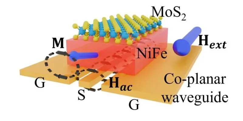
Recent explorations into the behavior of molybdenum disulfide (MoS₂) have illuminated its capacity to streamline energy use within magnetic memory films. By introducing a layer of large-area MoS₂, researchers are observing a significant reduction in energy loss, a factor that has long hindered the advancement of memory technologies. This dampening of energy dissipation is directly linked to the creation of a cleaner interface between the MoS₂ and the magnetic layer. This pristine interface is key, as it minimizes the subtle internal structural changes and associated energy waste that typically occur.
The implications of this reduced energy loss are far-reaching, pointing towards a future of more capable and efficient computing. Such advancements could enable:
Higher Density Memory: The capacity to store more data within the same physical footprint.
Energy-Efficient Computing: A considerable decrease in power consumption, crucial for devices ranging from portable electronics to extensive data processing centers.
Potential for Spintronics: MoS₂'s role in minimizing energy loss may finally help unlock the long-held promise of spintronics, a field aiming to utilize electron spin in addition to its charge.
Synthesis and Device Performance
The viability of this approach hinges on the practicalities of creating and integrating these MoS₂ layers. Investigations have detailed methods for synthesizing MoS₂ films using techniques like atomic layer deposition (ALD), a process noted for its potential commercial scalability. This ALD approach, when applied to materials such as Aluminum Nitride (AlN), has shown success in enabling high-performance MoS₂ field-effect transistors through strain engineering. Further work has involved the development of integrated circuits built upon bilayer MoS₂ transistors, alongside studies examining the electrical characteristics of single-layer and multilayer MoS₂ transistors, particularly concerning hysteresis and contact materials. The capability to produce MoS₂ on a wafer scale, as demonstrated in some research, underscores the move towards practical applications.
Read More: Linux users struggle to get older AMD GPUs working with new drivers
Background on Magnetic Memory and MoS₂
Magnetic memory devices rely on manipulating the magnetic orientation of thin films to store data. However, the process of switching these orientations can be energy-intensive, leading to heat generation and wasted power. This inefficiency has been a persistent bottleneck in increasing storage density and reducing the power draw of electronic devices.
Read More: HKUST Scientists Discover How DICER Enzyme Cuts RNA With High Precision in 2024
Two-dimensional materials, like MoS₂, have emerged as materials of interest due to their unique electronic and physical properties. In this context, MoS₂ acts as an intermediary layer. Its introduction at the interface of the magnetic film appears to smooth out irregularities that typically cause energy loss during magnetic switching. While the primary focus here is on energy reduction in magnetic memory, the broader field of 2D materials research continues to explore their utility in various electronic components, including transistors and sensors. Previous studies have also looked at how MoS₂ interfaces affect other properties of magnetic heterostructures, such as perpendicular magnetic anisotropy and spin-orbit torque.


.jpg)

