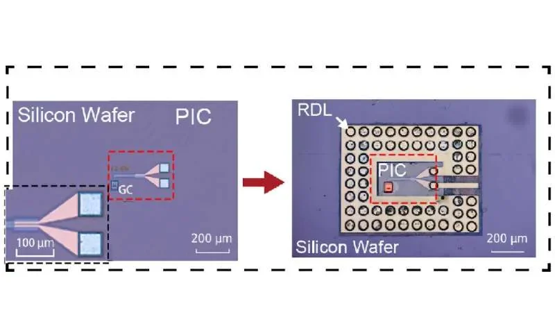
Researchers led by Dr. Wei Chu have demonstrated a reconfigurable germanium-silicon (Ge-Si) photodetector capable of achieving data transmission speeds of 336 Gbps. Published recently in Advanced Photonics Nexus, the study addresses the bottleneck in AI-driven data centers by utilizing a low-loss integration strategy known as fan-out wafer-level packaging (FOWLP).
| Performance Metric | Achievement |
|---|---|
| Transmission Rate | 336 Gbps |
| Packaging Strategy | Fan-out wafer-level (FOWLP) |
| Core Material | Germanium-Silicon (Ge-Si) |
| Key Structural Component | Heterogeneous Redistribution Layer (RDL) |
Engineering for Signal Integrity
The transition to higher bandwidths in server-to-server communication is currently obstructed by physical limitations in electronic-photonic integration. Traditional manufacturing methods frequently suffer from signal degradation and physical space constraints, preventing the density required by modern machine learning workloads.
The approach employed by Dr. Chu’s team relies on a heterogeneous redistribution layer designed to mitigate these losses:
Grounded Coplanar Waveguides (CPWG): Used within the RDL stack to maintain signal fidelity across high-speed interconnects.
FOWLP Integration: By moving away from conventional assembly, the team reduced the signal path complexity, effectively scaling interconnect density.
Reconfigurable Architecture: The photodetector’s adaptability allows for stable signal detection across diverse communication environments, addressing the stability-to-speed trade-off often found in high-speed communication systems.
Background and Context
The rapid expansion of large language models necessitates a fundamental rethink of how data centers move information. As of May 19, 2026, the reliance on optical interconnects is total, yet the physical manufacturing processes for these components have struggled to keep pace with the power and speed requirements of newer hardware clusters. By optimizing the link between photonic detection and electrical routing, this work attempts to bridge the gap between legacy packaging constraints and the requirements of future high-performance computing clusters.
Read More: Amazon and Argos cut Final Fantasy VII Rebirth price to £43.99
The study confirms that the use of an RDL stack allows for high-quality signal detection without the typical trade-offs in energy efficiency.