New interconnect strategies involving light are emerging to circumvent the entrenched limitations of High Bandwidth Memory (HBM) for advanced AI processors. This shift signifies a departure from purely physical stacking of memory chips, aiming to unlock substantially greater memory capacity and data transfer speeds crucial for the escalating demands of artificial intelligence workloads.
The core challenge is the "memory wall," a persistent bottleneck where memory speed fails to match the rapid gains in processing power. Traditional methods of increasing HBM capacity, primarily through stacking more DRAM dies vertically, are encountering physical and manufacturing limits. Pushing stack heights beyond current levels, such as 12 or 16 layers, leads to exponential increases in process difficulty and risks exceeding specified height limitations. Even the relaxation of these standards by bodies like JEDEC highlights the diminishing returns of vertical expansion.
Read More: AI Faked Evidence Against Korean Actor, Police Say
Decoupling and Bridging the Gap
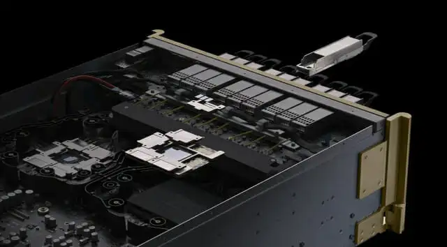
The emergent solution proposes a fundamental re-architecting: decoupling the Graphics Processing Unit (GPU) from its adjacent HBM and bridging the increased physical distance with optical signals. This approach abandons the long-held principle of co-locating components for minimal data transfer time. Instead, by strategically spacing the GPU and HBM, and using light to transmit data, the constraints imposed by the GPU's physical perimeter, termed its "shoreline," are overcome. This spatial liberation allows for significantly more HBM to be placed laterally around or beneath the GPU, potentially increasing total memory capacity and bandwidth by several fold.
Discussions are underway regarding optimal placement strategies, with options ranging from utilizing the immediate area around the GPU to dedicating a separate zone beneath the GPU board. This latter approach could necessitate changes to the overall form factor of GPU assemblies, potentially extending the motherboard lengthwise.
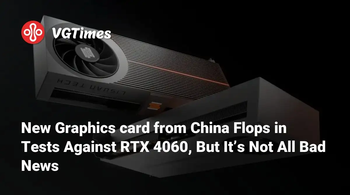
Read More: Lisuan LX 7G100 GPU Performance vs RTX 4060 as of May 2026
Industry Scrutiny and Technical Hurdles
The move toward optical interconnects is not confined to theoretical discussions. Memory makers are actively engaging with customers to explore these solutions, with researchers confirming preliminary talks with partners for next-generation AI accelerators. The outsourced semiconductor assembly and test (OSAT) sector is keenly observing this trend, with an executive predicting that larger-scale optical connections, such as rack-to-rack and server-to-server links, will precede chip-level integrations, though the pace of optical research suggests this transition could be swift.
While the underlying principles mirror established data center optical networking, the miniaturization of optical conversion technology to the microscopic scale required for intra-board chipsets presents a significant technical barrier. The successful implementation hinges on developing optical components that are not only smaller but also boast higher integration densities to operate within confined board spaces.
Read More: GameSir G7 Pro Controller Memorial Day Sale 2026 Price and Features
The Evolving AI Hardware Landscape
This pursuit of breaking the memory wall is intertwined with broader industry developments. The upcoming HBM4 standard, for instance, is expected to feature faster interfaces, higher input/output counts, and improved power efficiency per bit. Foundries like TSMC are playing an increasingly central role, collaborating with memory manufacturers such as SK Hynix and Micron on HBM4 and HBM4E respectively.
Beyond HBM, innovations in silicon photonics are also contributing. Companies are developing chiplets that offer substantial optical bandwidth, enabling chip-to-chip communication and potential memory expansion. Architectures are being explored that allow for disaggregating AI compute from memory, fostering shared memory pools.
Furthermore, the demand for higher interconnect speeds is driving advancements like Tower Semiconductor's new architecture, which utilizes an 8-lane configuration delivering 200Gbps per lane, a significant increase over previous 100G lane setups. These developments underscore a dynamic market where specialized solutions are being forged to meet the insatiable computational needs of AI. The development also signals a greater reliance on foundries for advanced packaging and component integration.
Read More: Why ASUS VA34VCPSR limits RTX 5080 performance on 23 May 2026